Tessent Multi-die software helps users dramatically speed and simplify critical design-for-test (DFT) tasks
As demand for smaller, more power efficient and higher performing Integrated Circuits (IC) continues to challenge the global IC design community, next-generation devices increasingly feature complex 2.5D and 3D architectures that connect dies vertically (3D IC) or side-by-side (2.5D) so that they behave as a single device. However, these approaches can present significant challenges for IC test, since most legacy IC test approaches are based on conventional two-dimensional processes.
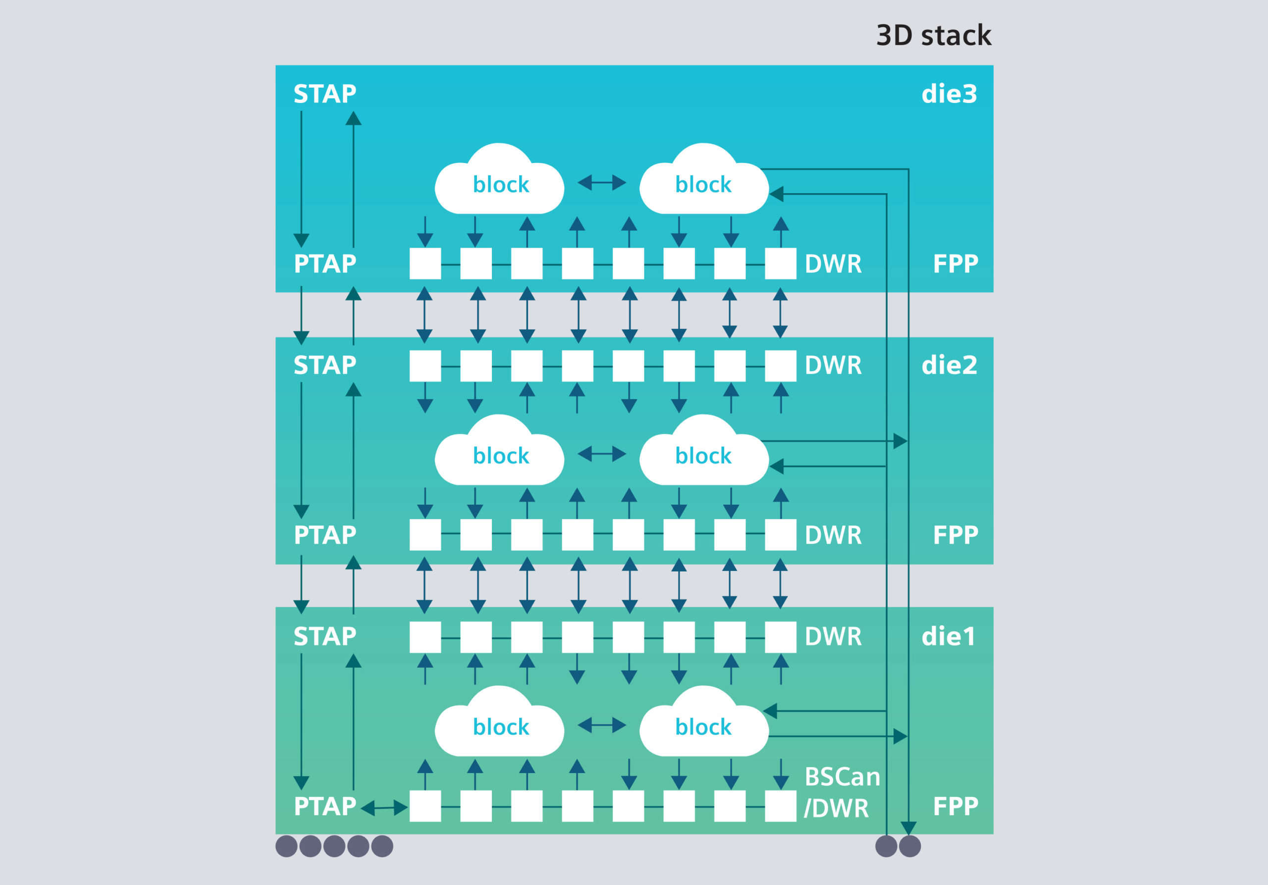
To address these challenges, Siemens has introduced its Tessent Multi-die software to automate DFT for highly complex tasks associated with 2.5D and 3D IC designs. Using Tessent Multi-die software, IC design teams can rapidly generate IEEE 1838 compliant hardware featuring 2.5D and 3D IC architectures.
IC designers are seeing dramatic spikes in IC test complexity due to the rapid adoption and deployment of designs featuring densely packed dies in 2.5D and 3D devices so the Tessent Multi-die software helps to reduce test implementation effort and simultaneously optimise manufacturing test costs. The software can also generate die-to-die interconnect patterns and enable package level test using the Boundary Scan Description Language (BSDL).
As traditional 2D IC design approaches reach their limit, more design teams are using the power, performance and form factor advantages that 2.5D and 3D IC architectures can deliver. But deploying these advanced schemes in new design starts without first establishing a DFT strategy that acknowledges the inherent challenges these architectures present can raise costs and undermine aggressive timelines. It’s therefore necessary to use evolving DFT technology.
- UK manufacturing steps up to COVID-19 crisis - April 2, 2020
- Clustering Innovation - March 12, 2020
- A Global Monitor - March 6, 2020

